
The largest time chunks in any product’s life cycle are in the design and engineering phases. This is because there are questions that need to be answered, both in how the product will perform and how the product itself will be made. Each of these parallel design inquiries are rooted in materials science, which at its basic level employs the evaluation and application of a material’s physical properties to make engineering decisions. Over the last 3 decades, shifts to digitization by the design and manufacturing worlds have contributed to the year-over-year advancements in the design loop. The use of finite element analysis (FEA) has revolutionized the way companies attack their structural designs; workstation processor speeds and high-end graphics cards have kept pace to give engineers in-depth knowledge of how their components react to service loads. In manufacturing, robots can repeatedly perform intricate machining, welding, or even build full components in the case of Additive Manufacturing (3-D Printing). However, the lynchpin between these design and manufacturing sectors, materials science, has remained a mostly analog endeavor. Relying on testing, measurement, and analysis, materials science has been necessarily slower in comparison.
The pivot to predictive, analytics-driven strategies is well underway in many industries and is certainly bearing fruit. In healthcare, forests full of patient information on paper have been digitized into electronic health records (EHRs), and health trends are now being predicted with astonishing accuracy. Even in the (slightly) less academic world of internet searches, aggregation of data (search terms, geographies, times of year, among others) reveals a very accurate picture of seasonal illness trends around the globe. The retail sector’s “loyalty card” programs may offer discounts for shoppers, but the habitual data received in return is much more valuable. Manufacturing’s use of the Big Data concept of IoT- Internet of Things (adapted to the Industrial Internet of Things – IIoT, a.k.a. Industry 4.0) is giving plant managers actionable data for improving production rates. Suddenly, the “necessarily slow” process of materials science has become a “cripplingly slow” bottleneck. The drumbeat for progress is persistent from all critical industries (aerospace, automotive, energy, medical devices, etc.). It is inevitable that the products and production methods of the future will demand a quantum leap in materials science. This leap will be facilitated by three main aspects: fundamental changes to materials science education, increasing reliance on desktop prototyping, and the maturation of Additive Manufacturing.
Materials Science Education
Using systematic numerical modeling to analyze and solve complex mechanics problems has been the basis of FEA techniques since their initial development in the late-1960s. The underlying math (algebraic matrices and differential equations) had been around for much longer than this, but the computational capability for solving anything more than the most basic geometries was realized only in the latter-half of the 20th century. It really is amazing how fast FEA has become entrenched in the design process for most industries, but not completely surprising given the amount of attention being paid to it at the university level. As FEA is a natural extension of math and computer science, you will often find entire courses in these disciplines being devoted to the finite element method. These courses place particular emphasis on using software as an assisting tool to visualize the problem (structural analysis, fluid dynamics, etc.). Mechanical engineering students are now required to have at least introductory-level knowledge of this method and one of its fundamental tenets: not every location on a component sees the same stress. On the other side of campus sits the materials science department. Aspiring engineers taking introductory materials courses are told to neglect the reality that materials are not homogeneous and isotropic (the same everywhere), and are also exposed to the physical tests used to assess material properties. Unlike their experience with finite element methods, students’ takeaway from materials science is that it is some kind of “black box” with parameters that are difficult to quantify; only upper-level students would understand. This type of thinking must change, as materials science undergoes the digital transformation necessary to keep up with industry.
Desktop Prototyping
Desktop prototyping goes hand-in-hand with FEA-assisted design. Engineers can rapidly assess the effects of loading components in different ways, or the effects of putting the same loads on components with different geometries. A vanguard of new technologies to digitize materials science is approaching critical mass; these form the basis of Integrated Computational Materials Engineering (ICME). VEXTEC’s VPS-MICRO® software is an ICME tool that efficiently marries quantifiable microstructural characteristics with FEA-supplied stresses, to visualize and predict the durability of a component, or even a system of components. Indeed, these material properties are not the “black box” many engineers imagine, nor are they the single deterministic values that are presented to them on material specifications and lot certification reports. These properties are now being leveraged computationally, to achieve efficient production rates and improved end-user performance. The efficient linkage of all of these digital methods to virtually prototype from “cradle to grave”, will give engineers and other decision-makers enormous capability in many aspects of their business (design, sustainment, warranty outlay, and supply chain, just to name a few).
Additive Manufacturing
Arguably, the two most prominent manufacturing buzzwords of the last 5 years have been “Additive Manufacturing” (AM). Companies have been investing heavily in these types of 3-D printing technologies that build components layer by layer, so much so that it has quickly become the third major manufacturing method for metallic components next to conventional forging and casting processes. Earlier this year, VEXTEC’s blog highlighted this shift in manufacturing, and how our VPS-MICRO® technology plays a key role in durability certification for AM. The benefits of additive are obvious: production of near-net shapes with intricate geometries, in controllable volumes with very little waste. However, unlike forging and casting, the materials science related to AM is not yet well-established. Industries are racing to find effective means of qualifying AM components, because the last thing anyone needs is a critical part made by AM to fail when it was not expected to. But the lure of the “on-demand production” that AM offers, much like “on-demand” taxi services like Uber and Lyft in the transportation service industry, will necessarily disrupt and pull materials science into the digital age.
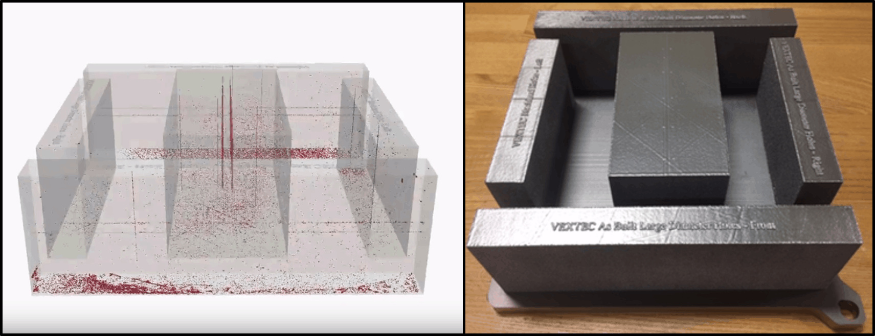
Digital visualization of additively-manufactured Ti-6Al-4V blocks (porosity highlighted in red), and the product as-built using electron beam melting (EBM).
Companies who embrace the analytical digitization of materials science will see outstanding returns both in the near-term and long-term, with technologies that can take full advantage of insatiable consumer demands, and with engineers who are better-equipped to adapt to those demands.


Leave A Comment